This is expected to reduce the chances of chip failures and improve the efficiency of electronic devices.
Ratan Tata is a well-known industrialist and philanthropist who led Tata companies including Tata Consultancy Services (TCS). The 86-year-old is now chairman emeritus of Tata Sons. He continues to contribute to society in many ways. Now his TCS has joined hands with IIT Bombay to build India's first advanced sensing tool for semiconductor chips. This is expected to reduce chances of chip failures and improve the efficiency of electronic devices, the company said on Tuesday.
Collaboration between TCS and IIT-Bombay to develop a quantum imaging platform for the non-destructive examination of chips is the first such initiative in India, the company said in a statement. "TCS has entered a strategic partnership with the IIT-Bombay, to develop India's first Quantum Diamond Microchip Imager. This advanced sensing tool will hold the potential to unlock new levels of precision in the examination of semiconductor chips and reduce chip failures," it said.
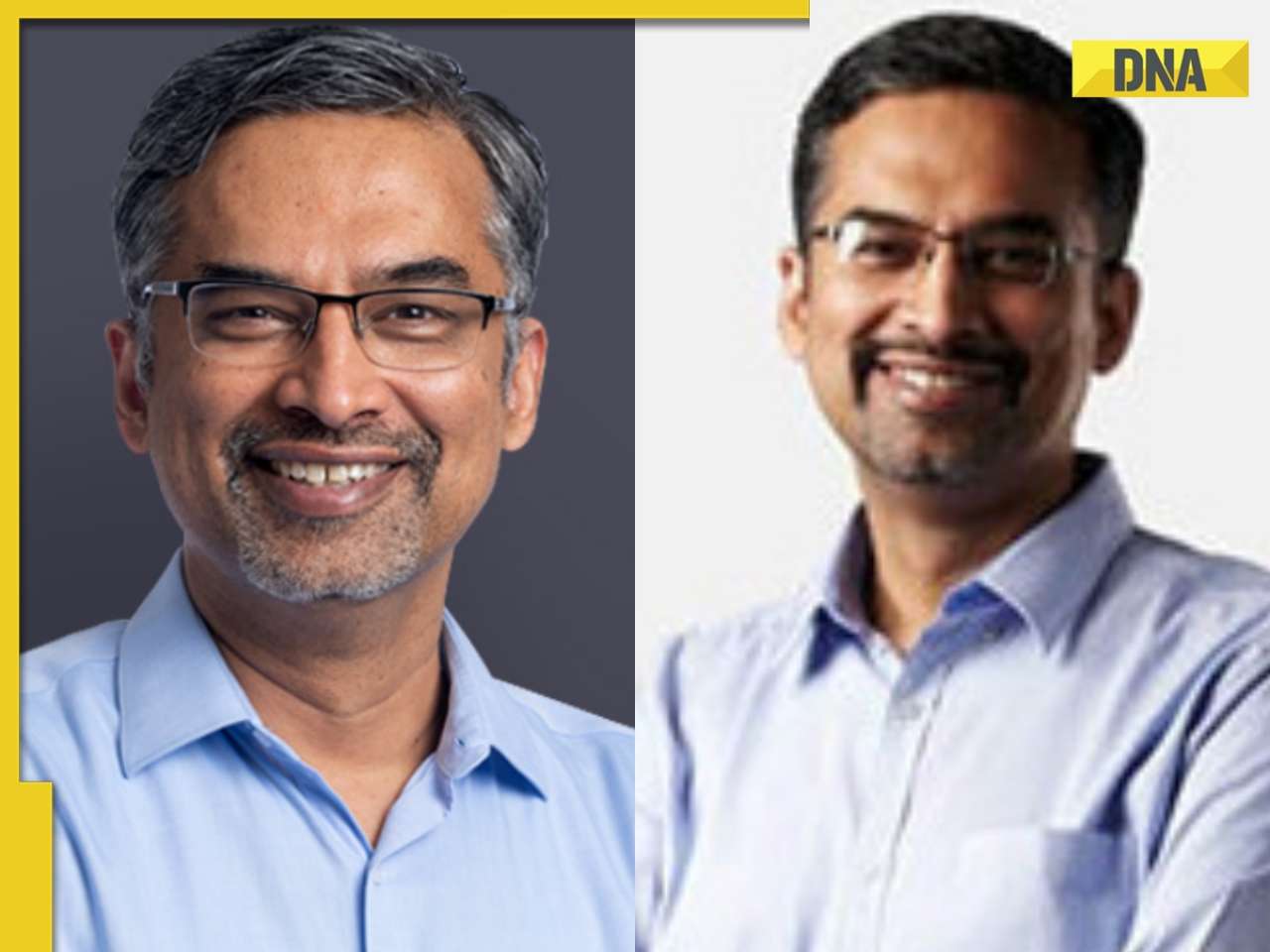
Over the next two years, experts from TCS will work with Kasturi Saha, Associate Professor in the Department of Electrical Engineering of IIT-Bombay to develop the quantum imaging platform in the PQuest Lab.
READ | Meet Indian genius who founded India's first pharma company, he is called 'Father of...
"PQuest group at IIT Bombay is excited to collaborate with TCS on developing a quantum imaging platform for the non-destructive examination of chips, leveraging our extensive expertise in quantum sensing to drive innovation. By working together, we aim to transform various sectors, including electronics and healthcare, and propel India forward through groundbreaking technologies,” Saha said.
The Quantum Diamond Microchip Imager can image magnetic fields that will enable a non-invasive and non-destructive mapping of semiconductor chips much like anI at a hospital. The imager uses the defects in a diamond's structure, known as Nitrogen-Vacancy (NV) centres, together with the other hardware and software for detecting and characterizing anomalies in semiconductor chips.
(With inputs from PTI)


 "Ratan Tata's TCS, IIT Bombay join hands to build India's first...")
)
)
)
)
)
)
)
)
)
)
)
)
)
)


)
)
)
)
)
)